
Why Copper AM Is Difficult - And How We Solve It
Pure copper presents two well-known AM challenges: high reflectivity at infrared wavelengths and very high thermal conductivity. The combination causes low energy absorption and rapid heat dissipation, which can lead to porosity and incomplete fusion in conventional fiber-laser systems.
Our solutions:
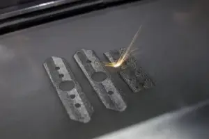
Green Laser (515 nm):
Higher copper absorption, enabling relative densities of ≥99.5% (typically 99.7–99.9%) and conductivity of 95–98% IACS in the post-processed state.
Validated Parameter Libraries:
Laser power 190–500 W, scan speeds 500–1250 mm/s, layer thickness 15–60 μm - qualified on internal benchmarks aligned with ASTM F3301 powder-bed fusion guidance.
Multi-Process Capability:
Copper LPBF (green-laser SLM/DMLS) and binder jetting platforms, matched to the application.
Manufacturing Processes
Choosing the right copper AM method depends on volume, precision requirements, and application:
|
Process |
Best For |
Key Characteristics |
|
Laser Powder Bed Fusion (LPBF / SLM) |
High-precision small-to-medium parts |
Finest resolution, ±0.1 mm typical, ideal for complex internal channels |
|
Binder Jetting (BJT) |
Mid-to-high-volume production, complex internal channels |
Lower cost per part at scale; requires debind and sinter steps |
|
Directed Energy Deposition (DED) |
Large parts and component repair |
High deposition rate; best for repair or cladding of high-value assemblies |
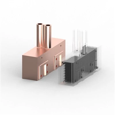
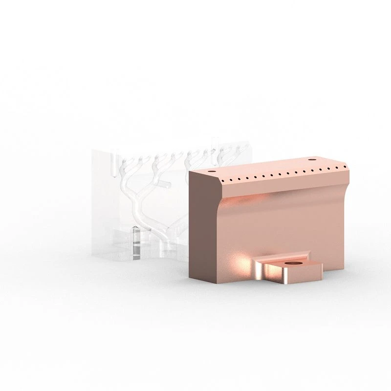
Recommendation: For applications dominated by complex internal channels - induction coils, compact heat exchangers, RF components - LPBF or binder jetting (depending on volume) is typically the best fit.
Material Properties
|
Property |
Pure Copper (3D Printed, Optimized) |
Beryllium Copper (BeCu) |
Brass (Typical) |
|
Electrical Conductivity (% IACS) |
95–98% |
15–45% |
26–28% |
|
Thermal Conductivity (W/m·K) |
~390 |
~105–230 |
~109–121 |
|
Tensile Strength (MPa) |
200–260 (HIP + annealed) |
410–1380 |
310–550 |
|
Density (g/cm³) |
8.9 |
8.3 |
8.4–8.7 |
|
Key Advantage |
Highest conductivity |
High strength |
Cost & machinability |
As-printed pure copper can be stronger (~300–350 MPa) but less conductive and less ductile; ranges above describe the recommended HIP + annealed delivery condition.
Post-Processing
Post-processing is essential to realize the performance of copper AM parts:
Hot Isostatic Pressing (HIP):
Closes residual microporosity; improves density and fatigue life with negligible impact on conductivity. Recommended for critical applications.
Annealing:
Relieves residual stress, restores ductility, and improves electrical conductivity. Typical 400–600 °C, atmosphere-controlled.
Vacuum Sintering (BJT only):
Achieves full density and target IACS conductivity after binder burnout.
Hydrogen / Inert-Atmosphere Annealing:
Relieves residual stress and improves ductility, reducing crack risk during thermal cycling.
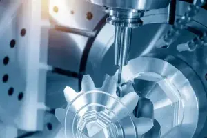
Precision CNC Machining:
Tightens tolerances and improves surface quality on mating features.
Surface Treatment:
Silver plating to reduce skin-effect losses at high frequencies; electroless nickel for corrosion resistance in harsh cooling-water environments.
Key Application Areas
|
Application |
Benefit of Copper AM |
|
Induction Coils |
Integrated conformal cooling channels, no internal brazed joints, ~2× longer service life (typical) |
|
Heat Exchangers |
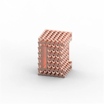
TPMS / lattice channels, 30–60% greater heat-transfer area vs. conventional designs |
|
RF / Microwave Waveguides |
Complex internal geometries reduce signal loss; used in satellite and radar systems |
|
Motor Winding Prototypes |
Rapid validation of advanced cooling structures for higher-efficiency motors |
|
Electrical Contacts |
Low resistance for high-current switching applications |
|
Medical & Industrial Parts |
Non-magnetic, high-conductivity custom components |
Technical Capabilities
Dimensional Accuracy: ±0.1 mm on typical features
Minimum Wall Thickness: 0.4–0.5 mm
Minimum Feature Size: 0.3–0.5 mm
Maximum Build Envelope: Up to 500 × 500 × 400 mm (process- and platform-dependent)
Material Purity: ≥99.9% Cu (ASTM B152 compliant)
FAQ
Hot Tags: copper additive manufacturing, China copper additive manufacturing manufacturers, suppliers, factory, 3D Printed Heat Exchangers, 3D Printed Induction Coils, Copper Additive Manufacturing, Industrial Metal 3D Printing, metal 3d printing, Pure Copper 3D Printing