
Technical Feasibility
Pure copper is challenging to laser-process because of its high reflectivity to near-infrared wavelengths and its very high thermal conductivity. These properties cause low energy absorption and rapid heat dissipation, which can lead to porosity and incomplete fusion in conventional fiber-laser SLM systems.
Our solutions
Green Laser (515 nm):
Markedly higher absorption in copper, enabling relative densities of ≥99.5% (typically 99.7–99.9% on validated geometries) and electrical conductivity of 95–98% IACS in the post-processed condition.
Validated Parameter Libraries:
Laser power 190–500 W, scan speeds 500–1250 mm/s, layer thickness 15–60 μm - qualified on internal benchmarks aligned with ASTM F3301 powder-bed fusion guidance.
Multi-Process Capability:
Copper LPBF (green-laser SLM/DMLS) and binder jetting platforms, matched to the application.
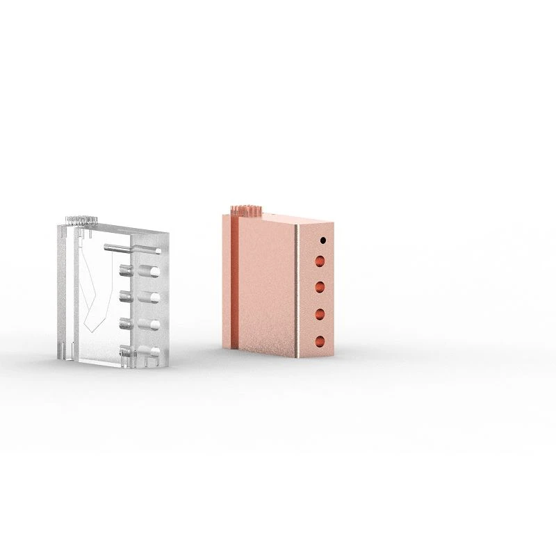
What Is Transparent Plastic Casting?
Manufacturing Process
Our pure copper 3D printing primarily uses Laser Powder Bed Fusion (LPBF). The process consists of:
Powder Preparation - High-purity (≥99.9%) gas-atomized spherical copper powder, particle size 15–45 μm, for good flowability and packing density.
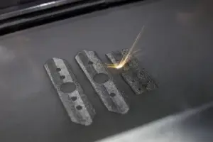
Laser Melting - Layer-wise green-laser scanning under an inert atmosphere (argon or nitrogen).
Layer-by-Layer Building - Typical layer thickness 20–50 μm.
Cooling and Removal - Controlled cooling to limit residual stress, followed by powder removal and initial cleaning.
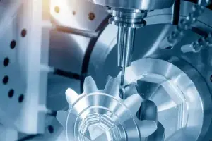
Post-Processing - HIP, annealing, CNC machining, and surface finishing as required
Dimensional capabilities:
- General accuracy: ±0.1 mm on small features; ±0.2% on larger dimensions
- Minimum wall thickness: 0.4–0.5 mm (design dependent)
- Minimum feature size: 0.3–0.5 mm after parameter optimization
Material Properties
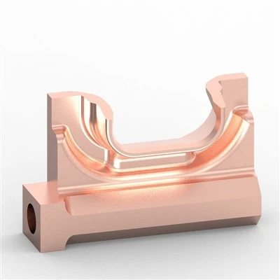
Properly post-processed 3D-printed pure copper retains the bulk-material properties expected of the alloy: electrical conductivity of 95–98% IACS, thermal conductivity ~390 W/m·K, density 8.9 g/cm³, and good ductility after annealing.
Copper vs. Common Alternatives
|
Property |
Pure Copper (3D Printed, Optimized) |
Beryllium Copper (BeCu) |
Brass (Typical) |
|
Electrical Conductivity (% IACS) |
95–98% |
15–45% |
26–28% |
|
Thermal Conductivity (W/m·K) |
~390 |
~105–230 |
~109–121 |
|
Tensile Strength (MPa) |
200–260 (HIP + annealed) |
410–1380 |
310–550 |
|
Density (g/cm³) |
8.9 |
8.3 |
8.4–8.7 |
|
Key Advantage |
Highest conductivity |
High strength |
Cost & machinability |
Tensile strength values reflect the HIP + annealed condition. As-printed copper can exhibit higher strength (up to ~350 MPa) but lower conductivity and ductility, and is generally not recommended as the delivered state for conductive applications.
For applications where electrical or thermal performance is the primary requirement, and extreme mechanical strength is not, pure copper additive manufacturing is typically the best material choice. With low porosity, the conductivity of LPBF copper closely approaches that of wrought copper.
Post-Processing Options
Post-processing is essential to realize the full performance of pure copper AM parts:
Hot Isostatic Pressing (HIP):
Closes residual microporosity and improves fatigue life with negligible impact on conductivity. Recommended for critical applications.
Annealing:
Relieves residual stress, restores ductility, and improves electrical conductivity. Typical range: 400–600 °C, atmosphere-controlled.
CNC Machining:
Tightens tolerances on mating features (down to ±0.01 mm) and improves surface quality.
Surface Finishing:
Electropolishing for low surface roughness (Ra typically <1.6 μm on accessible surfaces); silver plating for reduced skin-effect losses at high frequencies; electroless nickel for corrosion resistance.
These steps can be combined per requirements. HIP + annealing is the standard combination for aerospace-grade components.
Application Scenarios

Induction Coils
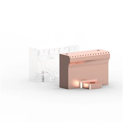
Monolithic construction with integrated conformal cooling channels eliminates failure-prone brazed joints. Conformal cooling supports more uniform temperature distribution and sustained higher-power operation. Field results from our customers indicate service-life improvements of roughly 2× over comparable brazed copper coils, with the exact gain depending on duty cycle and coolant conditions.

Heat Exchangers / Heat Sinks
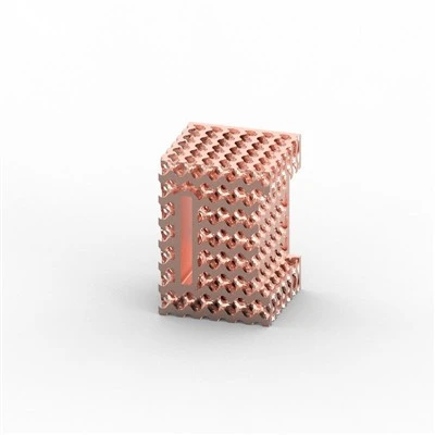
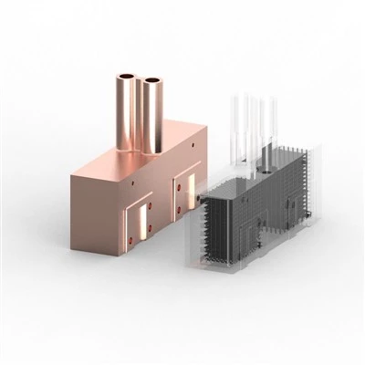
Complex internal flow channels - TPMS lattices, spirals, and wavy plates - increase surface-area-to-volume ratio and promote turbulent mixing, improving thermal performance. Widely used in electronics cooling and new-energy systems.
Electrical Contacts
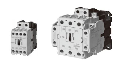
High conductivity supports low contact resistance for high-current switching applications.

RF / Microwave Waveguides
Complex internal geometries reduce signal loss in satellite communication and radar systems while enabling lighter assemblies.
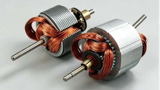
Motor Winding Prototypes
Rapid validation of advanced cooling structures and hairpin/profile-wire concepts for higher-efficiency motors.

Medical & Industrial Custom Parts
Customized non-magnetic or high-conductivity components for specialized equipment.
FAQ
Hot Tags: pure copper 3d printing, China pure copper 3d printing manufacturers, suppliers, factory, 3D Printed Heat Exchangers, 3D Printed Induction Coils, Copper Additive Manufacturing, Industrial Metal 3D Printing, metal 3d printing, Pure Copper 3D Printing