
Precision & Assembly Matching
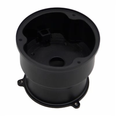
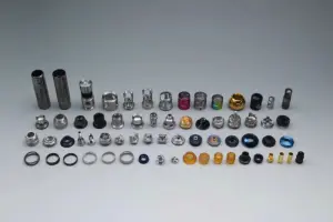
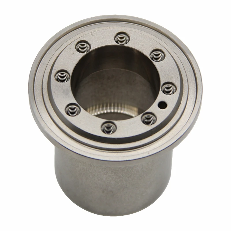
In electronic product development, first-time fit rate is critical. We focus on precision machining tailored to real assembly scenarios - ensuring PCB mounting holes, connector interfaces, and shielding cavities align correctly on the first try, reducing iteration and assembly issues.
Positional Tolerances for PCB Mounting Holes
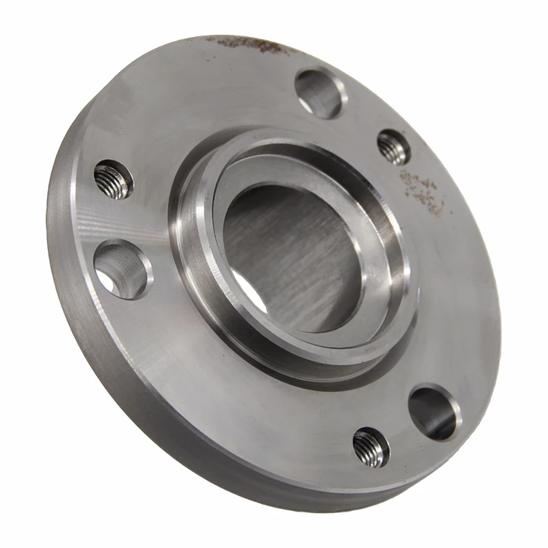
Using unified datums and deviation-compensation strategies, we typically hold hole-diameter tolerance of ±0.02 mm and positional tolerance of ±0.05 mm (Ø position-tolerance zone), supporting stress-free PCB installation. Tighter values can be quoted on request.
Connector Interface Matching - Flanges, Threads & Mating Surfaces
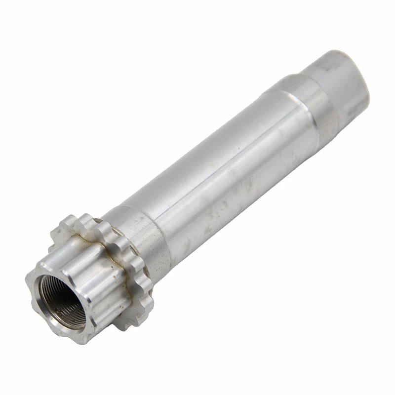
Precision machining for RF, D-SUB, M12, and similar connectors. We hold ISO 965 6H/6g thread fits and coaxiality within 0.02 mm on critical features for reliable signal transmission and mechanical mating.
CMM Inspection & First-Article Reports
100% CMM inspection on critical dimensions with detailed FAI reports provided for first articles - meeting the traceability requirements of electronic OEMs.
Tolerance Capability Comparison
|
Feature |
General Machining (ISO 2768-mK) |
Our Capability |
Notes |
|
Hole diameter tolerance |
±0.1 mm |
±0.02 mm |
Higher first-time fit rate |
|
Hole position tolerance |
±0.1–0.2 mm |
±0.05 mm |
Tighter alignment for connectors |
|
Thread fit |
ISO 965 6H/6g |
ISO 965 6H/6g |
Reliable and consistent |
|
Flatness (sealing surface) |
0.05–0.1 mm |
0.02 mm |
Better EMI sealing performance |
Reference standard updated to ISO 2768 (general machining tolerances); previous reference to IPC-2222 was incorrect - IPC-2222 covers PCB design rather than CNC tolerances.
EMI / EMC Requirements
EMI/EMC performance depends heavily on the structural integrity and electrical continuity of machined parts. We engineer enclosures that help your product pass FCC Part 15, EN 55032, and similar EMC tests.
EMI Shielding Enclosure Machining
Strict gap control (apertures kept well below λ/20 at the highest frequency of concern) and reliable conductive continuity between mating surfaces. Capabilities include complex multi-cavity shielding structures with verified grounding paths.
Gasket Groove Precision for EMI Sealing
Gasket-groove tolerances controlled to within ±0.05 mm to achieve target compression. We work with beryllium-copper finger stock, conductive elastomers, and conductive foam, and tune groove geometry to each gasket type.
Ground-Plane Continuity - Surface-Treatment Considerations
We help you choose between conductive surface treatments (chemical conversion coatings such as alodine/chromate, conductive anodizing, electroless nickel) and standard insulating anodizing. Selecting the wrong treatment is a frequent cause of grounding failures in EMI designs - we flag this risk during DFM.
Material Selection
We recommend materials based on functional needs - thermal management, EMI shielding, insulation, environmental resistance - rather than price alone.
Aluminum Alloys - 6061-T6 & 6063 for Enclosures
6061-T6 offers good strength and machinability with thermal conductivity ~167 W/(m·K), well-suited to RF module housings and heatsink bases. 6063 typically anodizes to a more uniform appearance for visible enclosures.
Copper & Brass - C101 / C360 for Electrical Contacts
C101 (oxygen-free electronic copper) achieves electrical conductivity of ~101% IACS, suitable for high-current contacts and busbars. C360 brass offers a balanced combination of conductivity and machinability for connectors and terminals.
Stainless Steel - 316L for Harsh Environments
Used in medical electronics, industrial control boxes, and marine applications. Its non-magnetic structure minimizes interference in EMI-sensitive designs.
Engineering Plastics - PEEK, POM, FR-4–Compatible Resins
Used for insulating components, connector bodies, and high-frequency substrate supports. UL 94 V-0 flame-retardant grades are available for applications requiring controlled flammability behavior.
Micro-Feature Machining
As electronic devices shrink, we deliver reliable micro-machining capabilities:
- Minimum feature size: minimum inner radius R0.3 mm, minimum wall thickness 0.3 mm (aluminum) / 0.5 mm (plastic), aspect ratio up to ~8:1
- Fine thread milling: M1.2 to M3 threads in aluminum - suitable for compact handheld devices and precision instruments
- Complex internal cavities: multi-cavity RF and microwave modules with cavity flatness ≤0.01 mm and tight corner-radius control to manage resonance behavior
- Tight-pitch hole patterns: minimum hole-to-hole spacing 0.8 mm; minimum hole diameter Ø0.5 mm with tight perpendicularity and positional accuracy
Surface Quality
In electronics, surface quality is functional, not just cosmetic:
Ra targets by function: Ra 0.8 μm for sealing surfaces, Ra 1.6 μm for general mating surfaces, Ra 3.2 μm for cosmetic surfaces
Flatness & parallelism: heatsink mounting surface flatness ≤0.02 mm to ensure uniform TIM thickness and lower thermal resistance
Burr-free finishing: critical to prevent shorts. Ultrasonic cleaning, electrolytic deburring, and cleanroom-grade packaging available.
Surface Treatments & Secondary Operations
Complete in-house finishing and secondary operations to simplify your supply chain:
Conductive surface treatments vs hard anodizing (Type III):
chromate / alodine conversion coatings preserve surface conductivity for EMI grounding; Type III anodizing offers high wear resistance but is electrically insulating. We define application boundaries clearly.
01
Electroless nickel plating:
uniform coating (typical ±2 μm), suitable for complex internal cavity walls.
02
Selective gold plating:
applied only on contact areas to control cost while maintaining low contact resistance.
03
Passivation, chromate & RoHS-compliant treatments:
full documentation for REACH and RoHS compliance.
04
Secondary operations:
heat-staked inserts, laser marking, silk-screening, and cleanroom packaging.
05
FAQ
Hot Tags: electronic CNC machining, China electronic CNC machining manufacturers, suppliers, factory, Delrin Machined Parts, Electronic CNC Machining, High Tolerance Milling, On demand CNC Machining, Plastic CNC Milling, Precision CNC Milling